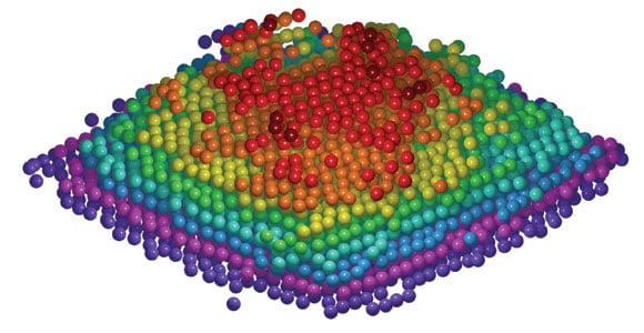
A team of physicists from UCLA have determined the three-dimensional positions of individual atoms for the first time, helping scientists better understand the structural properties of materials.
Atoms are the building blocks of all matter on Earth, and the patterns in which they are arranged dictate how strong, conductive or flexible a material will be. Now, scientists at UCLA have used a powerful microscope to image the three-dimensional positions of individual atoms to a precision of 19 trillionths of a meter, which is several times smaller than a hydrogen atom.
Their observations make it possible, for the first time, to infer the macroscopic properties of materials based on their structural arrangements of atoms, which will guide how scientists and engineers build aircraft components, for example. The research, led by Jianwei (John) Miao, a UCLA professor of physics and astronomy and a member of UCLA’s California NanoSystems Institute, is
published September 21 in the online edition of the journal Nature Materials.
For more than 100 years, researchers have inferred how atoms are arranged in three-dimensional space using a technique called X-ray crystallography, which involves measuring how light waves scatter off of a crystal. However, X-ray crystallography only yields information about the average positions of many billions of atoms in the crystal, and not about individual atoms’ precise coordinates.
“It’s like taking an average of people on Earth,” Miao said. “Most people have a head, two eyes, a nose, and two ears. But an image of the average person will still look different from you and me.”
Because X-ray crystallography doesn’t reveal the structure of a material on a per-atom basis, the technique can’t identify tiny imperfections in materials such as the absence of a single atom. These imperfections, known as point defects, can weaken materials, which can be dangerous when the materials are components of machines like jet engines.
“Point defects are very important to modern science and technology,” Miao said.
Miao and his team used a technique known as scanning transmission electron microscopy, in which a beam of electrons smaller than the size of a hydrogen atom is scanned over a sample and measures how many electrons interact with the atoms at each scan position. The method reveals the atomic structure of materials because different arrangements of atoms cause electrons to interact in different ways.
However, scanning transmission electron microscopes only produce two-dimensional images. So creating a 3-D picture requires scientists to scan the sample once, tilt it by a few degrees and re-scan it — repeating the process until the desired spatial resolution is achieved — before combining the data from each scan using a computer algorithm. The downside of this technique is that the repeated electron beam radiation can progressively damage the sample.
Using a scanning transmission electron microscope at the Lawrence Berkeley National Laboratory’s Molecular Foundry, Miao and his colleagues analyzed a small piece of tungsten, an element used in incandescent light bulbs. As the sample was tilted 62 times, the researchers were able to slowly assemble a 3-D model of 3,769 atoms in the tip of the tungsten sample.
The experiment was time-consuming because the researchers had to wait several minutes after each tilt for the setup to stabilize.
“Our measurements are so precise, and any vibrations — like a person walking by — can affect what we measure,” said Peter Ercius, a staff scientist at Lawrence Berkeley National Laboratory and an author of the paper.
The researchers compared the images from the first and last scans to verify that the tungsten had not been damaged by the radiation, thanks to the electron beam energy being kept below the radiation damage threshold of tungsten.
Miao and his team showed that the atoms in the tip of the tungsten sample were arranged in nine layers, the sixth of which contained a point defect. The researchers believe the defect was either a hole in an otherwise filled layer of atoms or one or more interloping atoms of a lighter element such as carbon.
Regardless of the nature of the point defect, the researchers’ ability to detect its presence is significant, demonstrating for the first time that the coordinates of individual atoms and point defects can be recorded in three dimensions.
“We made a big breakthrough,” Miao said.
Miao and his team plan to build on their results by studying how atoms are arranged in materials that possess magnetism or energy storage functions, which will help inform our understanding of the properties of these important materials at the most fundamental scale.
“I think this work will create a paradigm shift in how materials are characterized in the 21st century,” he said. “Point defects strongly influence a material’s properties and are discussed in many physics and materials science textbooks. Our results are the first experimental determination of a point defect inside a material in three dimensions.”
The study’s co-authors include Rui Xu, Chien-Chun Chen, Li Wu, Mary Scott, Matthias Bartels, Yongsoo Yang, and Michael Sawaya, all of UCLA; as well as Colin Ophus of Lawrence Berkeley National Laboratory; Wolfgang Theis of the University of Birmingham; Hadi Ramezani-Dakhel and Hendrik Heinz of the University of Akron; and Laurence Marks of Northwestern University.
This work was primarily supported by the U.S. Department of Energy’s Office of Basic Energy Sciences (grant DE-FG02-13ER46943 and contract DE-AC02—05CH11231).
Reference: “Three-dimensional coordinates of individual atoms in materials revealed by electron tomography” by Rui Xu, Chien-Chun Chen, Li Wu, M. C. Scott, W. Theis, Colin Ophus, Matthias Bartels, Yongsoo Yang, Hadi Ramezani-Dakhel, Michael R. Sawaya, Hendrik Heinz, Laurence D. Marks, Peter Ercius and Jianwei Miao, 21 September 2015, Nature Materials.
DOI: 10.1038/nmat4426
1 Comment
Does this mean that one could change the measuring electron beam from being slightly below the energy threshold where damage occurs to being slightly above so as to “move” W atom x,y,z to position x+1,y,z ?