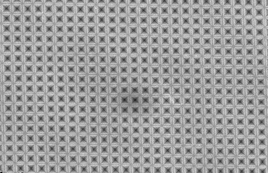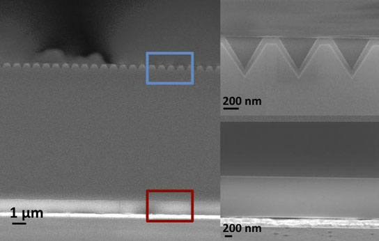
By using a pattern of tiny inverted pyramids etched into the surface of silicon, engineers at MIT found a new technique for building silicon solar cells that can trap rays of light as effectively as conventional solid silicon and reduce the thickness of the silicon used by more than 90 percent.
Highly purified silicon represents up to 40 percent of the overall costs of conventional solar-cell arrays — so researchers have long sought to maximize power output while minimizing silicon usage. Now, a team at MIT has found a new approach that could reduce the thickness of the silicon used by more than 90 percent while still maintaining high efficiency.
The secret lies in a pattern of tiny inverted pyramids etched into the surface of the silicon. These tiny indentations, each less than a millionth of a meter across, can trap rays of light as effectively as conventional solid silicon surfaces that are 30 times thicker.
The new findings are being reported in the journal Nano Letters in a paper by MIT postdoc Anastassios Mavrokefalos, professor Gang Chen, and three other postdocs and graduate students, all of MIT’s Department of Mechanical Engineering.
“We see our method as enhancing the performance of thin-film solar cells,” Mavrokefalos says, but it would actually work for any silicon cells. “It would enhance the efficiency, no matter what the thickness,” he says.

Graduate student Matthew Branham, a co-author of the paper, says, “If you can dramatically cut the amount of silicon [in a solar cell] … you can potentially make a big difference in the cost of production. The problem is, when you make it very thin, it doesn’t absorb light as well.”
The operation of a solar cell occurs in two basic steps: First, an incoming particle of light, called a photon, enters and is absorbed by the material, rather than reflecting off its surface or passing right through. Second, electrons knocked loose from their atoms when that photon is absorbed then need to make their way to a wire where they can be harnessed to produce an electrical current, rather than just being trapped by other atoms.
Unfortunately, most efforts to increase the ability of thin crystalline silicon to trap photons — such as by creating a forest of tiny silicon nanowires on the surface — also greatly increase the material’s surface area, increasing the chance that electrons will recombine on the surface before they can be harnessed.
The new approach avoids that problem. The tiny surface indentations — the team calls them “inverted nanopyramids” — greatly increase light absorption, but with only a 70 percent increase in surface area, limiting surface recombination. Using this method, a sheet of crystalline silicon just 10 micrometers (millionths of a meter) thick can absorb light as efficiently as a conventional silicon wafer 30 times as thick.
That could not only reduce the amount of expensive, highly purified silicon needed to make the solar cells, Mavrokefalos explains, but also cut the weight of the cells, which in turn would reduce the material needed for frames and supports. The potential cost savings are “not only in the cell material, but also in the installation costs,” he says.
In addition, the technique developed by Mavrokefalos and his colleagues uses equipment and materials that are already standard parts of silicon-chip processing, so no new manufacturing machinery or chemicals would be required. “It’s very easy to fabricate,” Mavrokefalos says, yet “it attacks big problems.”
To create the tiny dents, the researchers use two sets of overlapping laser beams to produce exceptionally tiny holes in a layer of material — called a photoresist — that is deposited on top of the silicon. This interference lithography technique is scalable to a large area. Following several intermediate steps, a chemical called potassium hydroxide is used to dissolve away parts of the surface that were not covered by the photoresist. The crystal structure of silicon leads this etching process to produce the desired pyramidal shapes in the surface, Mavrokefalos says.
So far, the team has only carried out the first step toward making the new type of solar cells, producing the patterned surface on a silicon wafer and demonstrating its improvement in trapping light. The next step will be to add components to produce an actual photovoltaic cell and then show that its efficiency is comparable to that of conventional solar cells. The expectation is that the new approach should produce energy-conversion efficiencies of about 20 percent — compared to 24 percent for the best current commercial silicon solar cells — but this remains to be proved in practice.
Chen, the Carl Richard Soderberg Professor of Power Engineering and director of MIT’s Pappalardo Micro and Nano Engineering Laboratories, says that if all goes well, the system could lead to commercial products in the near future.
Chen says the idea was developed after analyzing a great variety of possible surface configurations in computer simulations, and finding the arrangement that showed the biggest potential improvements in performance. But many teams around the world are pursuing a host of approaches to improving solar-cell performance using different materials, manufacturing methods, and configurations.
“It’s hard to pick a winner,” he says, but this approach has great promise. “We are pretty upbeat that this is a viable approach.”
Yi Cui, an associate professor of materials science and engineering at Stanford University, says this work produced “very exciting results. … The potential practical impact of this work could be significant, since it provides an effective structure for photon management for enabling thin cells.”
Cui says that since the expense of the silicon material “contributes significantly to the cost of solar cells,” developing thin silicon solar cells which can still absorb photons efficiently “is important for reducing the cost.”
Reference: “Efficient Light Trapping in Inverted Nanopyramid Thin Crystalline Silicon Membranes for Solar Cell Applications” by Anastassios Mavrokefalos, Sang Eon Han, Selcuk Yerci, Matthew S. Branham and Gang Chen, 21 May 2012, Nano Letters.
DOI: 10.1021/nl2045777
The work, which also involved postdocs Sang Eon Han and Selcuk Yerci, was supported by the U.S. Department of Energy’s Sunshot Program and by the National Science Foundation.
1 Comment
very good